Minimum effort GAL programming
This document describes how to program the GAL chips 16V8/A/B/C/D/Z/ZD, 18V10/B, 20V8/A/B/Z, 20RA10/B, 20XV10/B, 22V10/B/C/Z, 26CV12/B, 6001/B, and 6002B from Lattice, National Semiconductors and STMicrosystems with minimal effort.
You need
IC socket matching GAL
some 4k7 resistors 0.25W
100nF ceramic capacitor
SubD 25 pin male connector
some 4" short patch cables
5V/250mA and adjustable 8.5-16.5V/20mA laboratory power supply
Pin assignment of the different GAL chips during programming
|
|
GAL |
16V8 |
18V10 |
20V8 |
22V10 |
6001 |
26CV12 |
|
|
1(2) |
VIL |
VIL |
VIL |
VIL |
VIL |
VIL |
|
|
2(3) |
EDIT |
EDIT |
EDIT |
EDIT |
EDIT |
EDIT |
|
|
3(4) |
RA1 |
RA3 |
RA1 |
P/V- |
VIL |
P/V- |
|
|
4(5) |
RA2 |
RA4 |
RA2 |
RA0 |
RA0 |
RA0 |
|
|
5(6) |
RA3 |
RA5 |
RA3 |
RA1 |
RA1 |
RA1 |
|
|
6(7) |
RA4 |
SCLK |
VIL |
RA2 |
RA2 |
RA2 |
|
|
7(9) |
RA5 |
SDIN |
VIL |
RA3 |
RA3 |
VCC |
|
|
8(10) |
SCLK |
STB- |
RA4 |
RA4 |
RA4 |
VIL |
|
|
9(11) |
SDIN |
SDOUT |
RA5 |
RA5 |
RA5 |
RA3 |
|
|
10(12) |
GND |
GND |
SCLK |
SCLK |
SCLK |
RA4 |
|
|
11(13) |
STB- |
VIL |
SDIN |
SDIN |
SDIN |
RA5 |
|
|
12(14) |
SDOUT |
VIL |
GND |
GND |
GND |
SCLK |
|
|
13(16) |
VIL |
VIL |
STB- |
STB- |
STB- |
SDIN |
|
|
14(17) |
VIL |
VIL |
VIL |
SDOUT |
SDOUT |
STB- |
|
|
15(18) |
VIL |
VIL |
SDOUT |
VIL |
VIL |
SDOUT |
|
|
16(19) |
VIL |
RA2 |
VIL |
VIL |
VIL |
VIL |
|
|
17(20) |
VIL |
RA1 |
VIL |
VIL |
VIL |
VIL |
|
|
18(21) |
RA0 |
RA0 |
VIL |
VIL |
VIL |
VIL |
|
|
19(23) |
P/V- |
P/V- |
VIL |
VIL |
VIL |
VIL |
|
|
20(24) |
VCC |
VCC |
VIL |
VIL |
VIL |
VIL |
|
|
21(25) |
|
|
RA0 |
VIL |
VIL |
GND |
|
|
22(26) |
|
|
P/V- |
VIL |
VIL |
VIL |
|
|
23(27) |
|
|
VIL |
VIL |
P/V- |
VIL |
|
|
24(28) |
|
|
VCC |
VCC |
VCC |
VIL |
|
|
25 |
|
|
|
|
|
VIL |
|
|
26 |
|
|
|
|
|
VIL |
|
|
27 |
|
|
|
|
|
VIL |
|
|
28 |
|
|
|
|
|
VIL |
PLCC28 pin numbers of DIL24 chips in paranthesis
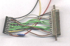
Wiring
Use 4k7 resistors to connect all VIL pins to the GND pin (we use 4k7 instead of the 10k mentioned in other documents, because some GALs have internal pull-ups of only 50k and illegal input states would occur using 10k resistors). Use 4k7 resistors to connect all other pins (including GND and EDIT) to the VCC pin to prevent open inputs during programming. Connect a 100nF ceramic capacitor between GND and VCC. If you use a GAL with built-in pull-ups, it is possible to go without the resistors, but I would not spare the 100nF capacitor and the pull-up on STB-. Do not try to program Normal GALs without the pull-ups on SCLK, SDIN, P/V, SDOUT, as the pulse rise time would be too slow without pull-ups to cope with the speed of the GALBlast program handling the LPT port.
Use short (max. length 4") wires to connect all pins mentioned below to the SubD 25 parallel printer port connector.
|
|
SubD25 pin |
GAL |
|
|
1 (/STB): |
STB- |
|
|
2 (D0): |
SDIN |
|
|
3 (D1): |
RA0 |
|
|
4 (D2): |
RA1 |
|
|
5 (D3): |
RA2 |
|
|
6 (D4): |
RA3 |
|
|
7 (D5): |
RA4 |
|
|
8 (D6): |
RA5 |
|
|
9 (D7): |
SCLK |
|
|
10 (/ACK): |
SDOUT |
|
|
17 (/SELIN): |
P/V- |
|
|
25 (GND): |
GND |
This arrangement was choosen so that an uninitialized port cannot affect the GAL.
Programming
Insert the GAL into the socket. Connect GND and VCC to the +5V output of a laboratory power supply. Connect GND and EDIT to an output of the power supply adjusted to +12V.
Launch the GALBlast program and select the parallel printer port used. Load the JEDEC file, the required GAL type should be automatically selected. Plug the SubD25 connector into the printer port, and issue the 'Write GAL' command. The PES of the GAL is read out and the required programming voltage will be displayed. Adjust the power supply to the required programming voltage (without overshoot, or disconnect first the SubD25, than the programming voltage, while adjusting) and continue with 'Write GAL'. Remove the SubD25 plug, turn off the programming voltage, turn off the power supply and remove the GAL from the socket.
--That's all --
Alternatives
If this method appears to risky, you may buffer the signals SCLK,RA0..RA5,STB-,P/V-,SDIN using two hex open collector driver ICs 7417 and 4k7 pull ups to VCC, and buffer SDOUT (4k7 pull up to VCC required) using the same chip before it connects to pin 17 (ACK-) of the parallel connector (4k7 pull up to +5V required). This way all GAL pins are electrically disconnected from the PC parallel port and the GAL may be turned off by removing VCC. Furthermore a D/A converter like the AD7524 can be used to select the programming voltage, if its inputs DB0..DB7 are connected to d0..d7 of the parallel port and WR- connects to pin 16 (FEED-), because the GALBlast program will output the required programming voltage (in 0.09375 volt increments if uncalibrated) to d0..d7 and pulls FEED- for a short time to L before ist starts talking to the GAL. Use an op-amp like the CA3140 to amplify the small output voltage (0 to 2.5V) to the required range (0 to 24V). The VCC power supply of the GAL may be controlled by a 5V SPST reed relay driven by INIT- of the parallel port, because the GALBlast program will take this line to L when it talks to the GAL.
AD7524
The AD7524 8 bit D/A converter from Analog Devices has been selected because it is wildely available and second sourced (MX7524 from Maxim, TLC7524 from Texas Instruments). The data sheet is available at http://www.analog.com/. The required reference voltage is generated using a 2.5V voltage reference like the LM336Z2.5 (data sheet at http://www.nsc.com). A 4n7 capacitor is used to filter spikes durings changes in the voltage setup completely to prevent the destruction of the GAL chip. You may use an other 8 bit latched DAC like the ZN428 (data sheet at http://www.mitelsemi.com/ under obsolete parts) which already contains the required voltage reference.
Power supply
The least number of parts are required if you use a regulated power supply delivering 24V at 250mA. The voltage only needs to be filtered using an electrolytic capacitor at the PCB. The op-amp will be powered directly from this voltage, a 7805 will regulate the +5V required for the remaining parts including VCC of the GAL. The 7805 will have to dissipate up to 5 watts and requires a heat sink to prevent overheating.
If you have no regulated power supply, you may supply unregulated +27..+35V, as are generated by using a 18V transformer, a bridge B40C250 (or 4 * 1N4004 diodes) and a filter capacitor of 1000uF/40V, and regulate the voltage at the PCB using a 7824. A 1N4004 series diode to protect the circuit from applying power in wrong polarity is not a bad idea.
If you don't want to dissipate 5 watts at the 7805, you may use a power supply of only 9V..12V, 250mA. The +24V programming voltage than has to be generated using a step up switching regulator.
LM78S40
Use a LM78S40 (or uA78S40) switching regulator with a 10nF timing capacitor and a 470uH/300mA storage coil suitable for switch mode converters and a 1R2 current limiting resistor. You will find the circuit and hints on construction in the data sheet available at http://www.nsc.com/. The LM78S40 is a good choice, because it already contains the required op-amp, but you may use a TL497 or other switching regulator and a separate op-amp (like the CA3140) instead.
If you want to use my predesigned circuit, look here