| Low Cost Function Generator
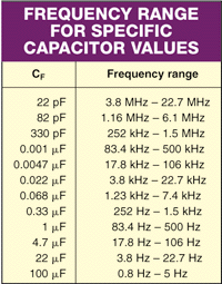
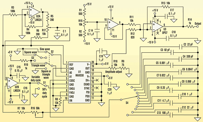
This was a design that we were going to do when time permitted but Electronic Design beat us to it. So, instead of reinventing the wheel, we present you with their implementation. by Ken Levine This low-cost function generator, based on the Maxim MAX038 high-frequency waveform generator, produces sine, triangle, and square waves from under 1 Hz to over 20 MHz (See figure Below). The frequency, amplitude, and offset of all output waveforms are adjustable, as is the duty cycle of the square wave. Frequency adjustment is accomplished with a capacitor bank and a variable resistor. Amplitude, offset, and duty-cycle adjustments are performed via variable resistors. Switches S2 and S3 select the waveform type to be generated. The frequency range is chosen using one of 12 capacitors, C2-C13, via switch S4. Resistor R16 is for fine-tuning. The fADJ pin of U1 is tied to ground through a 12k resistor, so the frequency of the waveform at U1-19 is f = 2(IIN/CF), where IIN = VREF/R, R is the sum of R7 and R16, and VREF = 2.5 V. The values of C2-C13, R16, and R7 were chosen to provide frequency-range overlap. Table 1 shows the frequency range for each capacitor value.
The output at U1-19 is 2 V p-p, centered around zero, for all waveforms. For amplitude adjustment, R18 and R9 form a voltage divider. The portion of U1-19 fed to the summing amplifier U3 varies from 0.74% to 100%. The summing amplifier multiplies this voltage by -12.2, so the signal at U3-6 will vary from 0.18 V p-p to 24.4 V p-p. The offset voltage is controlled by resistor R15. This voltage is fed to the summing amplifier, where it's added directly (the gain through the summing amp is 1) to the waveform voltage. Resistors R1 and R2 force the variation in the offset voltage to be within 13.6 V to +13.6 V to prevent the unity-gain buffer amplifier from being overdriven. Duty-cycle adjustment is controlled by resistor R17. The +2.5-V reference voltage of U1 is passed through a unity-gain inverter to R5. R5, R17, and R6 (which is tied to the +2.5-V reference voltage) form a voltage divider. The voltage developed across R17 varies from 2.3 V to +2.3 V. It first goes through a unity-gain buffer, then to the DADJ pin of U1. This ensures that the voltage at DADJ falls within the operating limits of 2.3 V to +2.3 V.
|