One of the unusual features of the out-of-production Programmable Drum Set was its use of touch switches for control. Like most touch switches, these detect the difference in the capacitance of a plate when it is being touched by a finger versus the parasitic capacitance of the plate alone.
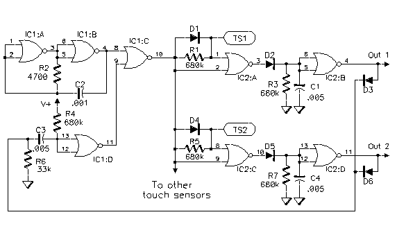
The capacitance added by touching the plate is detected using a square
wave oscillator. In the diagram below IC1:A and IC1:B, two gates from a
4001 CMOS Quad NOR IC, form an astable multivibrator with a 50kHz
frequency as determined by the time constant of R2 and C2. The square wave
output is buffered by IC1:C and used to drive a group of touch switches.
Only two switch plates - TS1 and TS2 - are shown in the illustration, but
in the PDS, 16 touch switches were excited by this one clock.
When the clock waveform is high, the capacitance of the sensing plate (TS2, for example) quickly charges through the forward biased diode D4 whether the pad is being touched by a finger or not. When the clock is low, the capacitor discharges through R5 and with no finger present the voltage quickly falls below the threshold required to switch IC2:C. Because of the inversion of the gate, it's output is a series of positive pulses at the clock frequency. The pulses quickly charge C4 through D5, but the C4 - R7 time constant is long enough that C4 can't discharge between pulses, so the output of IC2:D (which is the "switch" output) is low when there is no finger on the pad.
A finger touching the pad dramatically increases its capacitance and the larger capacitance cannot discharge through R5 fast enough to allow IC2:C to switch, so its output pulses go away and its output stays low. With the charging pulses gone, C4 soon discharges through R7 and when its voltage falls below the threshold of IC2:D, this gate's output switches high, which represents the switch being "on".
Some touch switch designs tend to be "bouncy", which is to say that they may toggle rapidly between "on" and "off" when the pad is in that gray area between touched and, uh ... untouched. This design gets rid of the "on" bounce with short delays before responding - a finger has to be on the pad for 1mS. or so before the output changes state.
To debounce the "off" cycle, the clock is turned off briefly when a switch is released. In the circuit above, diodes D3 and D6 and resistor R6 form an OR circuit that causes the voltage across R6 to be high when any output is high. This voltage goes low when a switch is released, causing the monostable comprising C3, R4 and IC1:D to produce a short pulse that momentarily kills the clock by gating it off in IC1:C. While the clock is stopped the switch will read as "off" even if the finger is pressed back on the pad.
This circuit is pretty forgiving of supply voltages. In the PDS it was run from a 6V battery but anything from 5V to 18V should work fine.
In the PDS, the touch pads were copper land areas about 1/4" X 3/4" etched on the edge of the circuit board that also mounted the rest of the electronics. The pads were covered with epoxy ink to protect them and also legend their function. It looked like this. In prototype form, the pads can be covered by a strip of cellophane tape. It's not a good idea to touch the bare plate with your finger because this can produce unreliable operation. Changes in the size of the pads may require adjustments of the time constants.
Disclaimer: I have not built this pressure sensitive touch switch circuit so it may have unforeseen problems - in the real world of design this often happens, at least to me. The idea exploits the fact that the capacitance produced by the finger on the pad is roughly proportional to the force of the finger on the pad.
The circuit shown below measures this change in capacitance and converts it to a Pulse Width Modulated signal. The clock shown in the drawing is the same clock used in the earlier touch switches, but it’s frequency may need to be adjusted up or down for best operation. The clock signal is coupled to the two inputs of a 4030 CMOS ExOR gate by R1 and R2. When no finger is touching the pad associated with R1, the parasitic capacitance at the two inputs is about the same so the clock signal is more or less the same at both inputs. Since an ExOR gate has a high output only when the two inputs are different, the output stays low even though the two inputs are clocking. As the finger is brought up to the pad and capacitance increases, the phase of the input to pin 1 (with the touch pad) begins to lag. As the two inputs get more different the output of the gate produces a pair of pulses (one on the leading edge of the clock signal and the other on the trailing edge) and the width of the pulses increases. R5 and C1 integrate this variable width pulse to extract it’s average dc value. This voltage is amplified by the voltage follower with gain consisting of IC1, R3 and R4 and is available as a Pressure Control Voltage.
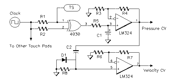
To get a Velocity Control Voltage - proportional to how fast the pressure changes - the Pressure CV is differentiated by C2 and R8. Assuming that the Pressure CV has been zero for some time, capacitor C2 will be completely discharged and there will be no current flow through R8 and consequently no voltage across it. As the Pressure CV increases, C2 begins to charge and this current produces a voltage across the resistor. Over the time that the pressure voltage is increasing there is a battle between how fast it rises and how fast C2 charges. If the CV rises rapidly, the charging current is high and the voltage across R8 is large. If the CV rises slowly, C2 can charge almost as quickly as it rises and the voltage across R8 remains small. The diode D1 clamps to ground the negative voltage produced across R8 when the finger is removed. Let’s be clear that the Velocity CV is a transient with peak amplitude proportional to velocity.
Here is how I will go about selecting component values when the time comes: R1 and R2 are going to be fairly high values, perhaps 680k and 470k respectively would be a good starting point. The only reason that their values would be different is to compensate for the additional parasitic capacitance that the touch pad represents beyond the capacitance of the traces, packaging and internal capacitance of the gate itself . Their values, and the frequency of the clock, are selected so that the output of the gate is low when no finger is on the pad and pulses appear and get wider as the finger is placed on the pad with increasing pressure. If there are pulses when there is no finger, probably R1 and R2 aren’t balance properly. If the pad is not sensitive enough probably the clock frequency needs to go up - if too sensitive, the Fc should probably go down. The size of the pad will effect these things also.
R5 and C1 will be chosen to provide the shortest time constant that will yield a fairly ripple-free voltage on C1. Probably 470k and .1uF would be a good starting point. R3 and R4 are chosen to boost the voltage on C1 to whatever you want for a max CV output - remember that the gain of this follower configuration is 1+(R4/R3).
The time constant for the differentiating C2 and R5 should be selected for maximum voltage across R5 when the pad is struck with maximum force. To short a time constant will result in pulse so narrow as to be unusable. Longer time constants make the Velocity CV simply follow the pressure voltage. I will probably start with 1uF and 47k values respectively. I’ll be surprised if the minimum available gain of 2 (when R6 and R7 are equal) is not really too much from the second buffer, since the Pressure CV has already been brought up to an optimal level. This stage will likely turn into a unity gain buffer by replacing R7 with a wire and eliminating R6.
If you play with this, or just have comments or questions please let me know by email at: honcho@paia.com


