Resistors (all 1/4 watt 5%)
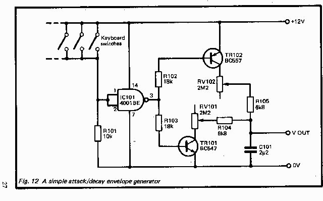
R101 10k
R102,103 18k
R104,105 6k8
Potentiometers
RV101,102 2M2 Lin
Capacitors
C101 2u2 miniature polyester
Semiconductors
IC101 4001BE
TR101 BC547
TrIO2 BC557
Miscellaneous
Circuit board
Two control knobs
14 pin DIL IC holder, wire etc.
ADSR Generator
Although an ADSR envelope shaper is rather more complex than an attack decay type, it does not greatly increase the cost of the synthesiser as a whole, and is probably well worth the additional expense. The block diagram of Figure 13 helps to explain the operation of the ADSR envelope generator featured here.
The flip/flop circuit operates two electronic switches, and the circuit is arranged so that when one of these s closed the other is open. This is very much like the system used in the attack/decay envelope generator described previously, and these two switches do in fact control the attack and decay phases of the envelope. Initially the attack switch is held open and the decay switch is closed, but when a key is operated this triggers a monostable multivibrator which generates a brief pulse. This pulse sets the flip/flop to its alternative state, so that the attack switch is closed and the decay switch is opened. The voltage on the storage capacitor then starts to rise, and it continues to do so until the charge potential reaches a certain threshold level. This is then detected by one of the voltage comparators which resets the flip/ flop to its original state. The storage capacitor then starts to discharge via the decay potentiometer, and it continues to do so, until a certain threshold level is reached. This level is detected by the second voltage comparator, and the sustain control enables the threshold level to be varied from zero to the peak envelope voltage. The voltage comparator cuts off the control signal to the decay switch, which is consequently opened, ending the decay phase.
There is a third electronic switch, the release switch, and this is operated from the keyboard switches via an inverter stage. This I
a key is released. Thus, when a key is released, the release phase of the envelope is commenced. A further gate and inverter stage are used to ensure that when the release switch is closed the attack switch must be open. This is necessary because there is otherwise a risk that both switches would be in the closed state if the key is released early in the envelope. This could result in the circuit hanging-up in an intermediate stale, rather than immediately entering the release phase.
The main circuit of the ADSR envelope shaper is shown in Figure 14, and the rest of the circuit appears in Figure 15.
The monostable and bistable (flip/flop) circuits are each formed from two of the CMOS 2 input NOR gates of IC9. 1C9a and IC9b are used in the monostable, while IC9c and 1C9d form the basis of the flip/flop. Both are conventional circuit configurations. C16 helps to avoid spurious triggering of the monostable due to contact bounce when a key is released C18 is the charge storage capacitor, while RV5 and RV6 are respectively the decay and attack controls.
1C10 is a dual operational amplifier, but in this circuit both sections act as voltage comparators. 1C10a is the one which resets the flip/flop at the end of the attack period, while 1C10b ends the decay period in conjunction with Tr2. RV7 is used to set the required sustain level. Tr5 is the release switch, and it is driven from the keyboard circuit via inverter Tr6. Tr7 are Tr8 are used to inhibit the attack circuit when a key is released.
I One problem with both the attack/decay and the ADSR envelope shapers is that they require an additional set of contacts on the keyboard. When using a proper keyboard there is riot usually any problem in having two sets of make contacts per key, but with a stylus keyboard there are obviously no switch contacts to trigger the envelope shaper. This problem is not insurmountable, and all that is needed is a simple trigger circuit of the type shown in the circuit diagram of Figure 16.
The circuit -is a voltage comparator, and it compares the keyboard voltage with a low reference potential of about 120 millivolts which is supplied by R101 and R 102. With no note being played, the non-inverting input of 1C101 is taken low by R103, and the output of the circuit goes low. When a note is played, the input voltage is more than 120 millivolts, and the output of the circuit goes high, triggering the envelope shaper. In fact the input voltage will only exceed 120 millivolts when the third or higher notes on the keyboard are played. In practice this means that the lowest two keys should be omitted, and the keyboard should start at "D" rather than "C".
R103 must have a high value so that the circuit does not significantly load the potential divider circuit in the keyboard circuit (which would cause the higher notes to sound flat). However, this makes the circuit prone to spurious triggering due to stray pick up of electrical noise in the lead to the stylus. To avoid this the lead should be kept reasonably short, and the stylus should be a type that ensures that the player is well insulated from the metal tip (the human body picks up substantial amounts of electrical noise from the environment).
ADSR Envelope Generator Components (Figs. 14 & 15)
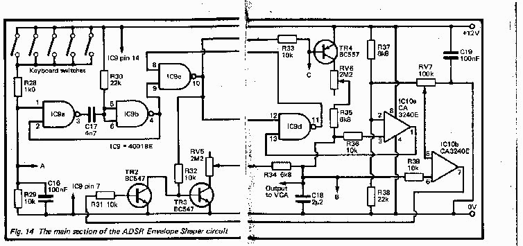
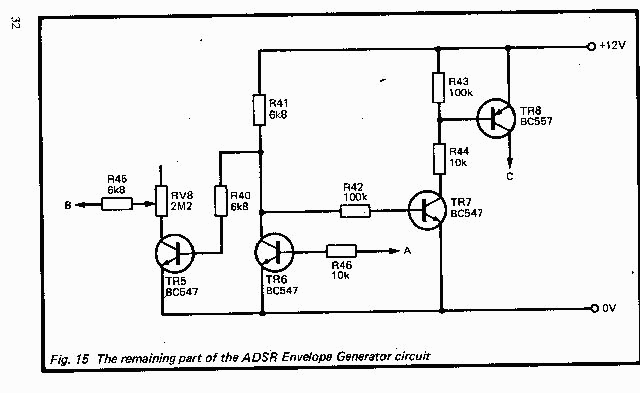
Resistors (all 1/4 watt 5%)
R28 lk
R29,31,32,33,36,39,44,46 10k
R30,38 22k
R34,35,37,40,41,45 6k8
R42,43 100k
Potentiometers
RV5,6,8 2M2 linear
RV7 100k linear
Capacitors
C16 100nF ceramic
C17 4n7 miniature polyester
C18 2u2 miniature polyester
C19 100nF ceramic
Semiconductors
1C9 4001BE
IC10 CA3240E
Tr2,3,5,6,7 BC547
Tr4,8 BC557
Miscellaneous
Printed circuit board
Four control knobs, IC holders, wire, etc.